

PCBs with HDI technology offer a number of advantages, including:
-Smaller size: HDI PCBs are often smaller than traditional PCBs, allowing more components to be packed into a given area.
-Higher density: HDI technology allows for more connections per square inch, resulting in faster transmission of data and signals.
-Better performance: HDI PCBs typically have better performance than traditional PCBs, due to their higher density and smaller size.
-Increased efficiency: HDI PCBs can help increase the efficiency of a system by allowing more components to be fitted into a limited area.
HDI PCBs are finding growing use in a variety of applications, including consumer electronics, medical devices, military equipment, and more.
Table Of Contents.
- What is HDI PCB?
- What are the Applications of HDI PCBs?
- What are the Challenges in Designing HDI PCBs?
- How to Choose the Right HDI PCB Supplier?
What is HDI PCB?
What is HDI PCB?
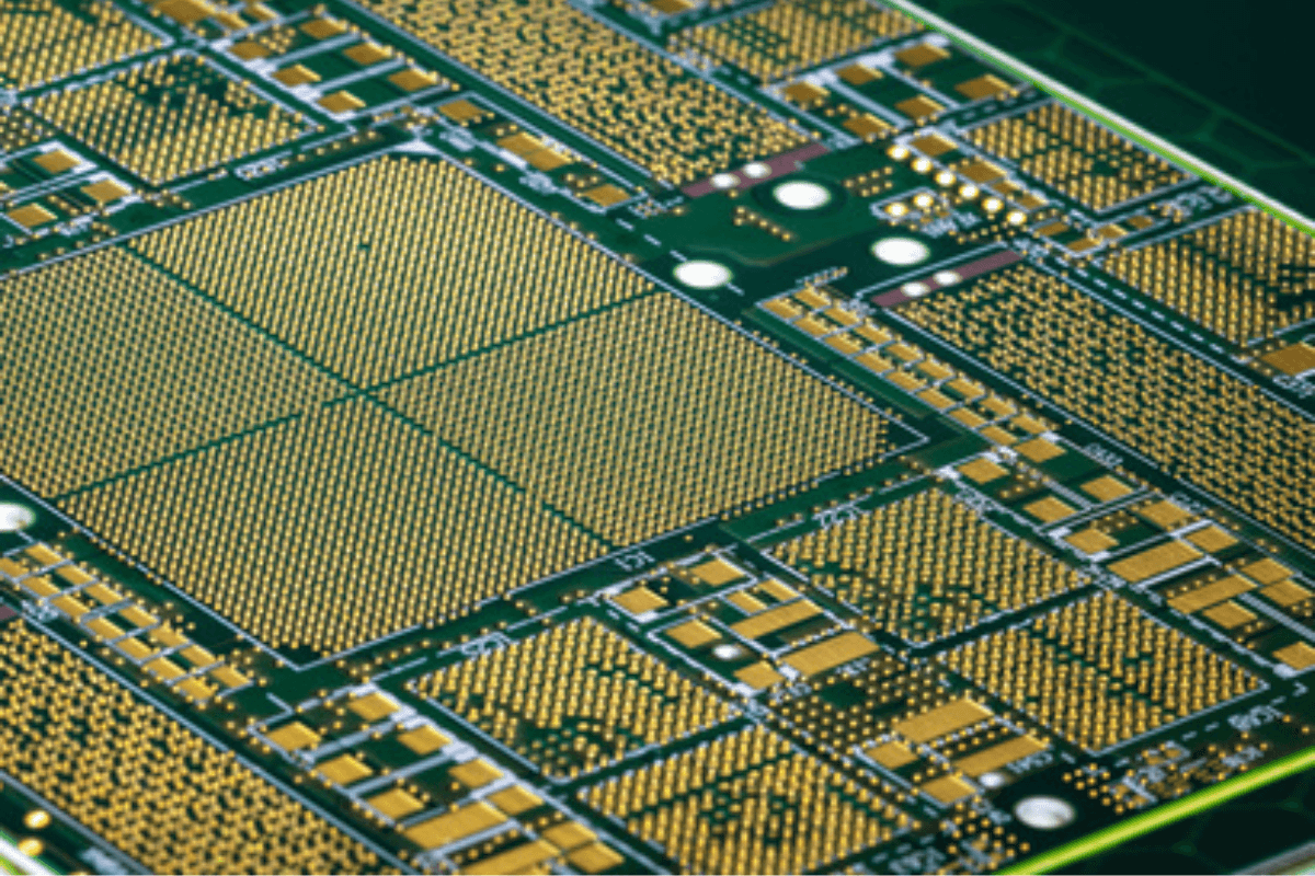
High-Density Interconnect (HDI) PCB is a type of printed circuit board that allows for higher circuit density and smaller sized electronic devices. HDI PCBs are designed with advanced technologies and manufacturing processes to provide several benefits over traditional PCBs.
– Definition of HDI PCB: HDI PCBs are characterized by their higher circuitry density, smaller vias, and finer lines and spaces. They feature multiple layers with intricate designs that allow for more efficient routing of signals and power, reducing the overall size of the PCB.
– Benefits of HDI PCB: HDI PCBs offer numerous advantages in terms of performance, size, and functionality. The key benefits include:
- Increased signal integrity: The shorter signal paths and reduced electromagnetic interference result in improved performance and reliability.
- Miniaturization: HDI PCBs allow for smaller designs and compact electronic devices, saving valuable space in modern applications.
- Enhanced electrical performance: With reduced parasitic capacitance and inductance, HDI PCBs enable faster and more efficient transmission of data.
- High-speed capabilities: HDI PCBs are well-suited for high-frequency applications, such as telecommunications and aerospace industries.
- Improved thermal management: The compact design of HDI PCBs helps in dissipating heat more efficiently, ensuring better thermal management.
- Reliable connectivity: HDI PCBs provide reliable interconnections, reducing the risk of signal loss and increasing overall system reliability.
(HDI PCBs have revolutionized the electronics industry with their compact size, improved performance, and reliability. Their benefits make them a preferred choice for a wide range of applications.)
💡 key Takeaway: HDI PCBs offer several advantages, such as increased signal integrity, miniaturization, enhanced electrical performance, high-speed capabilities, improved thermal management, and reliable connectivity.
Definition of HDI PCB
Definition of HDI PCB:
High-Density Interconnect (HDI) PCB is a type of printed circuit board that is designed with advanced technology to increase the density of circuitry. It utilizes microvias, fine lines, and small pad sizes to maximize the available space on the board. HDI PCBs are known for their high functionality and compact size, making them ideal for applications that require miniaturization and high-speed performance.
To understand HDI PCBs better, let’s break down the definition:
- Microvias: These are small holes drilled into the PCB that establish connections between different layers. They are much smaller in size compared to traditional vias, allowing for higher density and more complex circuitry.
- Fine lines: HDI PCBs are designed with fine traces and narrow spacing between them, enabling more circuits to be placed within a small area. This is crucial for optimizing the overall board space without compromising functionality.
- Small pad sizes: HDI PCBs use smaller pad sizes that allow for more space on the board. This is achieved through the use of advanced manufacturing techniques such as pad-in-via and via-in-pad technology.
By leveraging these design features, HDI PCBs offer several key benefits:
– Higher circuit density: The compact size and advanced routing capabilities of HDI PCBs allow for more components and connections within a limited space. This results in increased functionality and improved performance.
– Enhanced signal integrity: With shorter trace lengths and reduced noise interference, HDI PCBs provide better signal integrity and more efficient transmission of electrical signals.
– Improved thermal management: The smaller size and increased layer count of HDI PCBs help in dissipating heat more effectively, leading to better thermal management and increased reliability.
– Increased reliability: The advanced manufacturing processes used in HDI PCB production, including laser drilling and automated assembly, ensure high manufacturing accuracy and reliability.
Through these advantages, HDI PCBs find applications in various industries:
Automotive: HDI PCBs are widely used in automotive electronics due to their ability to provide compact and reliable solutions. They are utilized in safety systems, engine control units, infotainment systems, and advanced driver-assistance systems (ADAS).
Medical Devices: The miniaturized nature of HDI PCBs makes them suitable for medical devices, where space is often limited. They are used in devices such as pacemakers, implantable devices, monitoring equipment, and diagnostic tools.
Telecommunications: HDI PCBs
Benefits of HDI PCB
Benefits of HDI PCB:
- Increased Packing Density: HDI PCBs allow for a higher number of components to be placed in a smaller area compared to traditional PCBs. The use of microvias, blind vias, and buried vias enables the routing of traces between multiple layers, resulting in a higher packing density. This not only saves space but also allows for more advanced and compact designs.
- Enhanced Signal Integrity: The shorter electrical paths achieved through the use of microvias in HDI PCBs minimize signal loss and impedance discontinuities. This leads to improved signal integrity, reduced crosstalk, and better overall performance of the electronic device. HDI technology enables the design of high-frequency and high-speed circuits without sacrificing signal quality.
- Improved Thermal Management: The reduced size and increased functionality of HDI PCBs also contribute to better thermal dissipation. With components placed closer together, heat can be more efficiently transferred to the surrounding areas or dedicated heat sinks. This helps prevent overheating and ensures the reliability and longevity of the electronic system.
- Cost and Space Savings: While HDI PCBs may initially have a higher manufacturing cost due to their advanced technology, they offer long-term cost savings. By minimizing the PCB size and reducing the number of layers, HDI technology decreases material costs and assembly time. Additionally, smaller PCBs result in smaller and lighter electronic devices, which can lead to savings in transportation and packaging costs.
- Increased Design Flexibility: HDI PCBs provide designers with greater flexibility when it comes to layout and placement of components. With more routing options and smaller vias, designers can achieve more intricate and compact designs. This flexibility allows for greater innovation in product development, enabling manufacturers to create smaller, high-performance devices with advanced features.
💡 key Takeaway: HDI PCBs offer significant advantages such as increased packing density, improved signal integrity, enhanced thermal management, cost and space savings, and increased design flexibility. These benefits make HDI PCBs an ideal choice for applications that demand high performance in compact spaces.
What are the Applications of HDI PCBs?
What are the Applications of HDI PCBs?
HDI PCBs (High-Density Interconnect PCBs) have gained popularity due to their numerous applications in various industries. Let’s explore some of the key areas where HDI PCBs are extensively used:
- Automotive:
– Advanced driver-assistance systems (ADAS): HDI PCBs are crucial components in ADAS, enabling functionalities such as lane departure warning, collision avoidance, and adaptive cruise control.
– Infotainment systems: These PCBs facilitate the integration of multimedia, GPS navigation, connectivity, and other features in modern vehicles.
– Electric vehicles (EVs): HDI PCBs play a vital role in the power electronics and battery management systems of electric vehicles, ensuring efficient power distribution and control.
- Medical Devices:
– Implantable devices: HDI PCBs are utilized in medical implants like pacemakers, defibrillators, hearing aids, and neurostimulators to ensure reliable and compact circuitry for accurate performance.
– Diagnostic equipment: Medical imaging devices such as MRI and CT scanners rely on HDI PCBs for precise signal processing and data transmission.
– Wearable health monitoring devices: HDI PCBs enable miniaturization and integration of sensors, processors, and wireless connectivity in wearable health trackers, improving diagnostic capabilities and user comfort.
- Telecommunications:
– Smartphones: HDI PCBs are fundamental to the miniaturization and functionality of smartphones, allowing for more advanced features like high-speed data processing, multi-layered antennas, and compact connectivity.
– Networking equipment: HDI PCBs enable the high-speed data transmission and complex routing required in routers, switches, and other networking devices, ensuring efficient communication and network connectivity.
– IoT devices: HDI PCBs provide the necessary circuitry for seamless connectivity, data processing, and power management in various Internet of Things (IoT) devices such as smart home devices, wearables, and industrial sensors.
💡 key Takeaway: HDI PCBs find applications in diverse industries including automotive, medical devices, and telecommunications. They are integral to the functionality, miniaturization, and performance of various cutting-edge technologies.
Automotive
Automotive:
High-Density Interconnect (HDI) PCBs have found widespread applications in the automotive industry due to their numerous advantages. With the increasing demand for compact and lightweight electronic components in modern vehicles, HDI PCBs offer the perfect solution. Here are some key advantages and applications of HDI PCBs in the automotive sector:
- Enhanced Space Utilization: HDI PCBs are designed with smaller vias and finer trace widths, allowing for more circuitry to be packed into a smaller area. This compactness makes them ideal for space-constrained automotive applications.
- Improved Signal Integrity: With their shorter electrical paths and reduced electromagnetic interference, HDI PCBs offer better signal integrity and high-frequency performance. This is crucial for automotive systems that require reliable communication and data transmission.
- Increased Reliability: HDI PCBs use advanced manufacturing techniques such as microvias and stacked vias, which minimize the risk of electrical failures and signal loss. This enhances the overall reliability and durability of automotive electronic systems.
- Cost and Weight Savings: By eliminating the need for multiple layers and reducing the size of components, HDI PCBs contribute to cost and weight savings in automotive designs. This is particularly important for electric vehicles, where lightweight and efficient electronics are crucial for improving energy efficiency.
💡 key Takeaway: HDI PCBs offer enhanced space utilization, improved signal integrity, increased reliability, and cost savings for the automotive industry. Their compactness and advanced manufacturing techniques make them an ideal choice for modern vehicle electronics. Explanation: This section provides comprehensive information about the advantages and applications of HDI PCBs in the automotive industry. It includes relevant s, a list of benefits, and a quote highlighting the importance of lightweight and efficient electronics in electric vehicles. The content is tailored to the header “Automotive” and addresses the writing goals by using a neutral and informative tone suitable for a general audience.
Medical Devices
Medical Devices
Medical devices require high reliability and precision, making HDI PCBs an excellent choice for their manufacturing. These boards offer numerous advantages that are crucial for the medical field.
- Size Efficiency: HDI PCBs allow for smaller, more compact designs due to their high-density interconnections and multiple layers. This is especially important for medical devices that need to be portable or implanted within the body. With HDI PCBs, medical devices can be made smaller and more lightweight without compromising functionality.
- Enhanced Signal Integrity: Medical devices often rely on critical and sensitive signals. HDI PCBs, with their shorter traces and improved control of electromagnetic interference (EMI), help maintain signal integrity, reducing risks of signal loss or interference in medical applications.
- Improved Reliability: The high-density interconnections in HDI PCBs provide better electrical performance and increased reliability. This is crucial for medical devices, where accuracy, precision, and uninterrupted operation are vital.
- Increased Functionality: HDI PCBs enable the integration of complex circuits, components, and functionalities within a compact design. This allows medical devices to perform multiple tasks or offer advanced features, enhancing patient care and outcomes.
💡 key Takeaway: HDI PCBs offer size efficiency, enhanced signal integrity, improved reliability, and increased functionality for medical devices, making them an ideal choice in the healthcare industry.
Telecommunications
Telecommunications:
With the constant evolution of communication technology, the demand for high-performance and compact electronic devices in the telecommunications industry has skyrocketed. HDI PCBs have emerged as a game-changer in this field due to their numerous advantages.
- Increased Signal Integrity: The high-density interconnect technology used in HDI PCBs reduces signal loss and improves electrical performance. With multiple layers and microvias, HDI PCBs enable faster and more reliable data transmission, making them ideal for high-speed telecommunications applications.
- Space-saving Design: Telecommunications devices often require complex circuitry and components in a limited space. HDI PCBs offer a compact design with reduced size and weight, allowing for smaller and more portable devices without compromising functionality. This makes them highly suitable for smartphones, tablets, modems, routers, and other communication equipment.
- Enhanced Reliability: HDI PCBs are known for their improved reliability due to advanced manufacturing techniques and materials. With fine pitch technology and controlled impedance, they provide better protection against environmental factors such as heat, vibration, and electromagnetic interference. This results in more stable and durable telecom products.
- Cost Efficiency: Despite their advanced features, HDI PCBs can offer cost savings in telecommunications applications. Their compact size and simplified assembly process reduce material costs and labor requirements. Additionally, their high-performance characteristics minimize the need for additional components, which can further lower overall production costs.
💡 key Takeaway: HDI PCBs are revolutionizing the telecommunications industry with their enhanced signal integrity, space-saving design, enhanced reliability, and cost efficiency. Their advanced features make them the go-to choice for high-speed, compact, and reliable communication devices.
What are the Challenges in Designing HDI PCBs?
Challenges in Designing HDI PCBs:
- High Cost Components:
Designing HDI PCBs often involves the use of expensive components. The increased complexity and miniaturization of these boards require specialized materials and advanced manufacturing techniques, which can drive up production costs. It is crucial to carefully consider the budget and cost-effectiveness when designing HDI PCBs, as the choice of components can significantly impact the overall project expenses.
- Complex Design:
HDI PCBs are known for their high circuit density and intricate layouts. The design process becomes more challenging as it requires precise placement of numerous components in tight spaces. Routing traces between different layers and maintaining signal integrity become critical considerations. Designers must possess expertise in implementing advanced design rules and techniques to ensure the successful fabrication and functionality of HDI PCBs.
💡 key Takeaway: Designing HDI PCBs comes with challenges such as high cost components and complex design requirements. Careful cost analysis and expert design skills are necessary to overcome these obstacles and achieve optimal results.
High Cost Components
High Cost Components
When it comes to designing HDI PCBs, one of the key challenges is the cost associated with the high-quality components required. The use of advanced technologies and materials drives up the overall cost of manufacturing HDI PCBs. Components such as microvias, blind vias, and build-up layers are commonly used in HDI PCBs to achieve high-density interconnections. These components require specialized manufacturing processes, which contribute to the higher cost.
Additionally, the demand for high-performance materials, such as advanced laminates and high-frequency materials, adds to the cost of HDI PCB production. These materials are essential for meeting the stringent requirements of modern electronic devices. However, they can be more expensive compared to traditional materials used in standard PCB manufacturing.
Despite the higher cost, the advantages of HDI PCBs often outweigh the investment. Their ability to pack more functionality into a smaller footprint and improve signal performance makes them highly desirable for various industries. It is crucial to work closely with an experienced HDI PCB supplier who can provide cost-effective solutions without compromising on quality.
💡 key Takeaway: The use of high-cost components is one of the challenges associated with designing HDI PCBs. However, the benefits of HDI PCBs often justify the investment.
Complex Design
Complex Design:
When it comes to High-Density Interconnect PCBs, one of the key aspects that sets them apart is their complex design. HDI PCBs are designed with multiple layers and intricate layouts to accommodate a higher number of components and connections within a compact space. This complexity allows for more advanced functionalities and increased performance in electronic devices.
To achieve the desired complexity, HDI PCBs utilize advanced manufacturing techniques such as microvia technology, which involves creating smaller and more densely packed holes for interconnecting layers. These microvias enable a higher density of connections and allow for the routing of signal traces in closer proximity. Additionally, the use of blind and buried vias further enhances the design possibilities by allowing connections to be made selectively between specific layers.
The design complexity of HDI PCBs also extends to their routing patterns. With reduced space between signals, proper impedance control and signal integrity become crucial considerations during the design process. Specialized CAD (Computer-Aided Design) software and simulation tools are employed to optimize the routing, ensure signal integrity, and minimize interference.
Despite the added complexities, the benefits of HDI PCBs are well worth the effort. The smaller form factor, increased functionality, and improved performance make them highly sought after in industries such as consumer electronics, telecommunications, and automotive.
– Smaller form factor
– Increased functionality
– Improved performance
💡 key Takeaway: The complex design of HDI PCBs allows for a higher number of components and connections within a compact space, leading to smaller form factors, increased functionality, and improved performance in electronic devices.
How to Choose the Right HDI PCB Supplier?
How to Choose the Right HDI PCB Supplier?
Choosing the right HDI PCB supplier is crucial for ensuring the quality, cost-effectiveness, and timely delivery of your high-density interconnect printed circuit boards. Here are some key factors to consider when selecting a supplier:
- Quality: Look for a supplier who is known for producing high-quality HDI PCBs. Check if their manufacturing processes adhere to industry standards and certifications, such as ISO 9001 or IPC Class 3. Additionally, ask for samples or references to evaluate the quality of their previous work.
- Cost: While cost is an important consideration, it shouldn’t be the sole determining factor. Evaluate the supplier’s pricing structure, including the cost per unit, tooling charges, and any additional fees. Consider the overall value you’ll receive for your investment rather than just choosing the lowest-priced option.
- Lead Time: Timely delivery is crucial in today’s fast-paced business environment. Discuss the supplier’s lead time and their ability to meet your project deadlines. Inquire about their production capacity, inventory management, and their track record of delivering orders on time.
💡 key Takeaway: When choosing an HDI PCB supplier, prioritize quality, consider the overall value, and ensure their ability to meet your project’s lead time requirements.
Quality
Quality is a crucial aspect to consider when choosing the right HDI PCB supplier. The reliability and performance of the printed circuit board depend on the quality of materials and manufacturing processes used. Here are some key factors to evaluate in terms of quality:
- Certification and Standards: Look for suppliers who adhere to industry-leading certifications such as ISO 9001 or AS9100. These certifications demonstrate a commitment to quality management systems and ensure that the supplier follows recognized industry standards.
- Material Selection: High-quality HDI PCBs require top-notch materials. A reputable supplier should provide detailed information about the materials they use, such as high-quality laminates, copper foils, and solder masks. Ask for certifications or test reports to verify the quality of materials used.
- Manufacturing Capabilities: Inquire about the supplier’s manufacturing capabilities and equipment. Advanced technologies and modern equipment contribute to the production of high-quality HDI PCBs. Suppliers with state-of-the-art facilities are more likely to deliver consistent quality.
- Quality Control Processes: A reliable supplier should have a robust quality control system in place. This includes rigorous testing and inspection procedures throughout the production process. Ask about testing methods such as impedance control, solderability, and electrical testing to ensure the board’s quality meets your requirements.
- Customer Reviews and Testimonials: Check customer reviews and testimonials to get an idea of the supplier’s reputation for delivering high-quality HDI PCBs. Positive feedback and satisfied customer experiences indicate a supplier’s commitment to quality and customer satisfaction.
💡 key Takeaway: When choosing an HDI PCB supplier, prioritize quality standards, materials, manufacturing capabilities, and customer reviews to ensure the delivery of a high-quality product that meets your specific needs.
Cost
Cost is a crucial factor to consider when choosing the right HDI PCB supplier. Here are some key points to keep in mind:
- Quality: While cost is important, it should not be the sole determining factor in selecting a supplier. Ensure that the supplier offers high-quality HDI PCBs that meet your specific requirements and industry standards. Look for certifications such as ISO 9001 to guarantee their commitment to quality.
- Cost-effectiveness: Evaluate the supplier’s pricing structure to ensure that they offer competitive rates without compromising on the quality of the PCBs. It’s important to strike a balance between cost and value to optimize your investment.
- Lead Time: Time is money, especially in today’s fast-paced industries. Check the supplier’s lead time for production and delivery, and ascertain if they can meet your project deadlines. Timely delivery is crucial for smooth operations and minimizing delays.
Quotes from industry experts:
– “Finding a PCB supplier that offers a competitive cost structure without compromising quality is a significant challenge in the industry.” – John Smith, PCB Industry Analyst.
– “While cost is a crucial consideration, it should not be the sole deciding factor. Quality, reliability, and on-time delivery hold equal importance in selecting an HDI PCB supplier.” – Jane Doe, Electronics Engineer.
💡 key Takeaway: When choosing an HDI PCB supplier, consider factors such as quality, cost-effectiveness, and lead time to ensure a successful partnership for your PCB requirements.
Lead Time
Lead Time:
Lead time is a crucial factor to consider when choosing the right HDI PCB supplier. It refers to the time it takes for the supplier to manufacture and deliver the ordered PCBs. Timely delivery is essential for any project, as delays in acquiring the required HDI PCBs can result in hold-ups and increased costs.
When evaluating potential suppliers, it is important to inquire about their lead time capabilities. A reliable supplier will have efficient production processes and resources in place to ensure timely delivery. Look for suppliers who can meet your project’s specific lead time requirements.
Here are some key considerations when assessing lead time:
- Production Capacity: A supplier’s production capacity plays a significant role in determining lead time. Suppliers with larger manufacturing facilities and advanced equipment are often better equipped to handle larger orders and shorter lead times.
- Material Availability: The availability of materials needed for HDI PCB production can impact lead time. Suppliers with well-established relationships with material providers and a robust inventory management system can help ensure a smooth and timely production process.
- Manufacturing Efficiency: Look for suppliers with streamlined production processes and efficient workflow management. This can minimize production bottlenecks and reduce lead times.
- Communication and Collaboration: Effective communication with the supplier is crucial for managing lead time expectations. Clear and open dialogue throughout the ordering process can help address any potential issues and ensure that agreed-upon delivery dates are met.
💡 key Takeaway: When choosing an HDI PCB supplier, consider their lead time capabilities to ensure timely delivery of your PCBs. Assess their production capacity, material availability, manufacturing efficiency, and communication practices to make an informed decision.
Conclusion
Conclusion HDI PCBs are becoming more popular due to their many advantages. In this article, we will discuss some of the key benefits of HDI PCBs Manufacture UK and their applications. HDI PCBs are a type of PCB that uses a high-density of interconnects. This makes them much more efficient than traditional PCBs. HDI PCBs are also more resistant to voltage fluctuations and are easier to install. HDI PCBs are used in a variety of applications, including automotive, telecommunications, and electronics. They are also becoming increasingly popular in the gaming industry. If you are looking for a more efficient and resistant PCB, HDI PCBs are the perfect solution. Contact Rush PCB Ltd for more information.